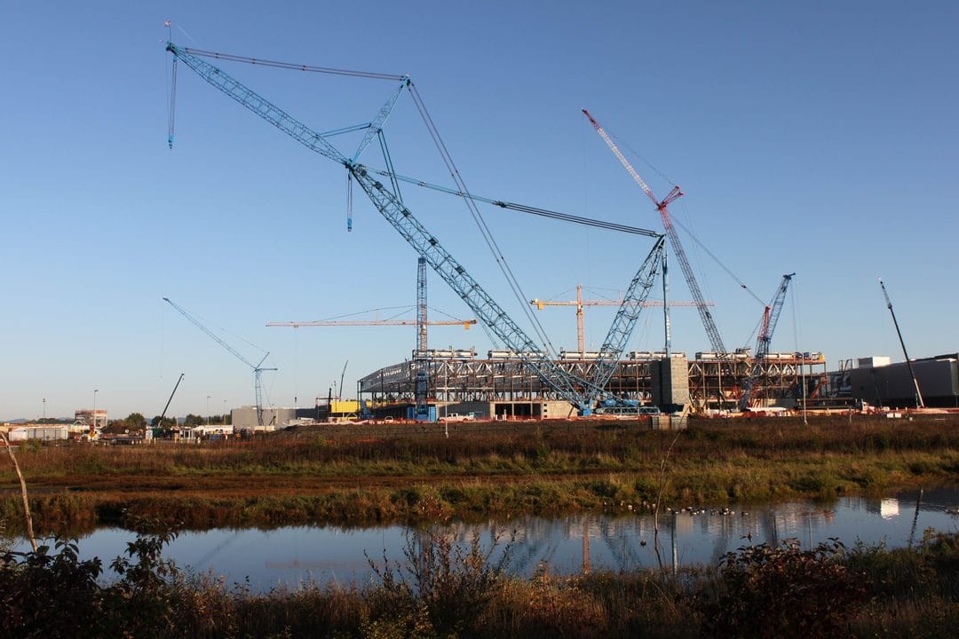
SK Hynix held a groundbreaking ceremony on Thursday, August 27, at Purdue University in West Lafayette, Indiana, formally launching construction of its first high-bandwidth memory (HBM) production base in the United States. The South Korean memory maker is putting more than $4 billion into the site, which will package and test the AI memory chips that feed Nvidia's most advanced accelerators. SK Hynix CEO Kwak Noh-Jung, Indiana Governor Mike Braun, US Senator Todd Young and Purdue President Mitch Daniels Jr. attended the ceremony at the university's Holloway Gymnasium.
A back-end plant, not a wafer fab
The Indiana campus will not manufacture DRAM wafers. SK Hynix plans to keep front-end wafer production in South Korea and ship the wafers to West Lafayette for stacking, packaging and testing into finished HBM modules — the advanced-packaging step that turns raw memory dies into the multi-layer stacks GPUs actually plug into. Construction on the physical site had quietly begun in April, months before Thursday's ceremony, with structural frames and columns already rising on the 540,000-square-meter plot.
SK Hynix expects the cleanroom to be ready by October 2028, with mass production of HBM4E — the successor to the HBM4 the company currently ships to Nvidia for the Vera Rubin platform — starting in the third quarter of 2029. Kwak said the site is designed to eventually reach annual output in the hundreds of thousands of wafers and become a core US HBM production base by 2030, though the company has been careful to frame that figure as a medium-term target rather than a near-term commitment. Roughly 1,000 people are expected to work at the site once it reaches full commercial operation.
CHIPS Act money, and a bigger political backdrop
The project originated in an April 2024 announcement pegged at $3.87 billion; SK Hynix now describes the total commitment as exceeding $4 billion. The US Department of Commerce, through the CHIPS and Science Act, has agreed to provide up to $458 million in direct funding plus $500 million in loans, according to figures published by the NIST CHIPS Program Office.
The ceremony landed against a broader push by Washington to pull memory-chip production onshore. Commerce Secretary Howard Lutnick visited Micron's fab construction site in Idaho last month to press the same point, and SK Group Chairman Chey Tae-won has said separately that his company is weighing additional US investment — potentially including a full memory fab — depending on whether power, water, labor and local supply-chain conditions line up. For now, the Indiana site remains back-end only, and Chey has not put a timeline on any decision.
Jobs, a Purdue partnership and a long supplier list
SK Hynix and Indiana officials put the direct employment figure at roughly 1,000 jobs once the plant is fully operational, with a wider estimate of about 7,000 direct and indirect jobs tied to construction and related supply-chain activity. The company signed a memorandum of understanding with Purdue University covering joint research on next-generation HBM and access to the school's engineering graduates, and it says more than 100 companies are currently being evaluated as local suppliers of materials, components and equipment for the site.
- Cleanroom completion targeted for October 2028
- HBM4E mass production targeted for the third quarter of 2029
- Roughly 1,000 direct jobs once fully operational — SK Hynix and Indiana officials cite about 7,000 total including construction and supply-chain roles, though that broader number depends on how many of the 100-plus prospective suppliers actually locate nearby
Why HBM is the chip everyone in Seoul, Hsinchu and Santa Clara is watching
HBM has become the bottleneck component of the AI buildout: without enough of it, GPU makers cannot ship finished accelerators no matter how much logic-die capacity is available. SK Hynix's HBM4 stacks up to 12 layers of DRAM in current production, and the company already produces higher-layer configurations for the successor generation. Nvidia's Vera Rubin platform is built around HBM4E, which is one reason SK Hynix wants a US packaging base close to its largest customer rather than shipping every finished stack from Korea.
The company used the same week to lay out where the underlying memory design goes after HBM4E. At the Hot Chips 2026 conference at Stanford University, SK Hynix presented iHBM, a design that embeds a dedicated thermal-conduction path inside the hottest area of the memory stack to cut heat resistance, and discussed hybrid bonding as the route to pushing HBM stacks past 20 layers. The company has said hybrid bonding will not appear in HBM4E — that technology arrives with HBM5 at the earliest, with volume production not expected before 2028. That roadmap work stays in Korea; West Lafayette packages whatever architecture ships from SK Hynix's Icheon and Cheongju sites, it does not design it.
Purdue's student newspaper, the Exponent, reported that rezoning-related lawsuits over the West Lafayette site were still working through the courts as of Thursday's ceremony, even as construction on the buildings themselves moves forward.