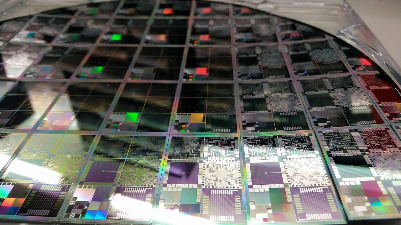
TSMC formally began volume production of its 2nm process node (internally N2) at the Fab 20 facility in Hsinchu Science Park on 24 April 2026, with the first commercial wafer-outs delivered to Apple in the first week of May. The ramp was three months ahead of the most aggressive analyst forecasts (Morgan Stanley's January 2026 note), and N2's defect density at production start was reported by TSMC at the Q1 earnings call as "comparable to N3E at equivalent ramp maturity" — translation: yields are tracking better than the previous node at the same point. Three observations from the technical and commercial dynamics now visible.
Why Apple, not Nvidia, got first allocation
The conventional analyst expectation through late 2025 was that Nvidia's next-generation GPUs (Rubin, replacing Blackwell Ultra) would dominate first-allocation queues at N2 given the AI capex cycle. The actual first-allocation customer is Apple, with the A20 SoC for the iPhone 18 family taping out in February and entering volume in May. The reasons are commercial rather than technical:
- Apple's wafer commitment for 2026-27 is 300,000+ N2 wafers per quarter, locked in through three-year minimum-take agreements signed in 2023. Nvidia's equivalent N2 commitment was made in late 2024 and is operationally smaller.
- Apple's chips are dramatically smaller and yield more dies per wafer. The A20 die at N2 is estimated at 90mm²; an equivalent Nvidia datacentre GPU die is 700-800mm². Even at the same defect density, Apple's per-wafer yield is far higher, making them economically optimal early-ramp customers.
- Apple paid up. The unconfirmed but widely reported pricing for N2 first-allocation wafers is roughly $30,000-$33,000 per wafer, against $20,000 for N3E. Apple's product margins absorb that; the second-tier customers couldn't justify it.
What this means for Nvidia and the AI pipeline
Nvidia's Rubin family is now confirmed for late Q3 2026 volume on N2 (specifically N2P, the performance variant), with announced shipping in H1 2027. The implication for AI capacity is that 2026 will see no significant generational performance jump in datacentre GPU compute — Blackwell Ultra runs the year. This is the technical reason behind the deceleration in AI capex growth that hyperscalers including Microsoft, Meta and Google guided to in their Q1 earnings calls. Not because demand has softened, but because the supply pipeline of fundamentally better silicon doesn't arrive until 2027.
The N2P yield surprise
Industry was expecting initial N2 yield in the 30-40% range and N2P (which uses additional EUV layers for higher performance) closer to 25-30%. TSMC's actual numbers, leaked through industry sources to DigiTimes and Semianalysis in early May, were 47% for N2 and 38% for N2P. Three factors contributed:
- EUV multi-patterning maturity: TSMC's experience from N3 with NA-EUV multi-patterning translated more directly than expected to N2.
- Backside power delivery (BSPDN): deferred from N2 to N2P. By isolating that complexity to the later process node, N2 itself looks more like a clean shrink of N3E.
- Apple's defect-tolerance design: Apple's M-series and A-series chips are designed with redundancy at the cache and core level that lets TSMC bin partially defective dies as lower-spec products. This is one of the structural reasons Apple is a desirable first-allocation customer.
What about Samsung Foundry's 2nm
Samsung's SF2 process, ramped at Pyeongtaek through Q1 2026, continues to have yield issues. Samsung's foundry division pivoted in March 2026 to a single-customer model on SF2 (likely Qualcomm's mid-tier mobile chip), effectively conceding the leading-edge race to TSMC for another full node generation. The gap between Samsung Foundry's SF2 and TSMC's N2 is now estimated at 4-6 quarters of effective maturity — the widest the leading-edge gap has been since 2020.
Three things to watch through Q3 2026
- TSMC Arizona N2 timeline: the Phase 3 facility was originally slated for 2028 production. Pressure from the US government to bring forward 2nm capacity domestically has been intense; expect a formal announcement of accelerated timeline at TSMC's July 2026 capex update.
- N2P yield trajectory: if N2P reaches 50% yield by Q4 2026 (the internal TSMC target), Nvidia Rubin volume guidance for 2027 looks credible. If it stalls at 40%, expect Nvidia revenue guidance cuts in the H1 2027 earnings season.
- Intel 18A: Intel's competing 2nm-equivalent process is in pre-production at the Ohio facility. Whether Intel can attract any meaningful external foundry customer for 18A — given TSMC's lead — determines whether the IDM2.0 strategy survives 2027.
The 2nm transition is the most consequential semiconductor process node since the FinFET introduction in 2011. The choices made in Q2 2026 about who gets allocation, at what yield, and at what price are shaping the AI infrastructure of 2027-2030.